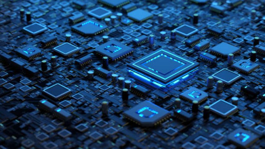

The creation of a modern microprocessor is a feat of engineering that involves dozens of sophisticated steps, carried out in ultra-clean environments using cutting-edge tools and atomic-level precision.
1. From Sand to Silicon
Silicon, the primary material in microprocessors, is derived from sand, specifically silicon dioxide. Through a chemical process known as the Czochralski method, pure silicon is extracted and grown into large, cylindrical single crystals called ingots. These ingots can weigh hundreds of kilograms and must be almost perfectly pure and defect-free.
2. Wafer Production
Once the ingot is ready, it is sliced into thin discs called wafers, typically about 0.75 mm thick. These wafers are then polished until they achieve a mirror-like surface, which is essential for the precise layering process that follows.
3. Photolithography: Drawing the Circuits
Photolithography is the process used to print extremely small patterns onto the wafer. First, the wafer is coated with a light-sensitive chemical called photoresist. A mask—essentially a stencil of the circuit design—is placed over the wafer. Then, ultraviolet (UV) light is shone through the mask. The light reacts with the photoresist, allowing specific parts to be chemically altered and later removed.
This process defines where the microscopic transistors and wires will be placed. Advanced microprocessors may go through this step dozens of times, with different masks, to build multiple layers of circuits.
4. Etching, Doping, and Layering
After exposure, the wafer undergoes etching, where unprotected parts are chemically removed to create the circuit patterns. Next, doping adds tiny amounts of elements like phosphorus or boron to change the electrical properties of the silicon. This is crucial to form transistors, which are the tiny switches that make up digital logic.
Layer after layer of transistors, metal interconnects (often made of copper), and insulating materials are deposited and etched. This vertical stacking of components allows billions of transistors to fit on a single chip, thanks to features smaller than 10 nanometers.
5. Inspection and Testing
Throughout the manufacturing process, the wafer is repeatedly inspected with electron microscopes and sensors to detect defects as small as a few atoms across. Once all the layers are complete, the entire wafer is tested using automated probes to identify functional chips.
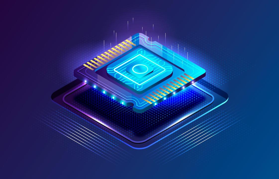
6. Dicing and Packaging
The finished wafer is cut—diced—into hundreds or thousands of individual microprocessors, called dies. Each die is then packaged: it is placed into a protective housing with metal contacts that allow it to interface with the rest of a computer system.
7. Final Testing and Distribution
Before shipping, each packaged chip undergoes another round of functional and thermal testing to ensure reliability under real-world conditions. Only those that pass all tests are sent to manufacturers, where they are installed into devices such as computers, smartphones, servers, and even cars.
Conclusion
Building a microprocessor is one of the most complex manufacturing processes ever developed. It combines materials science, nanotechnology, and precision engineering in facilities that cost billions of dollars. The result is a chip no larger than a fingernail, capable of performing billions of operations per second.